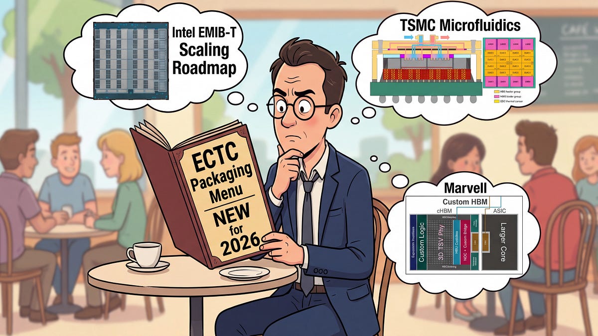
Marvell's custom HBM leaves the DRAM dies untouched and replaces the base die with one on an advanced logic process, pulling the memory interface off the accelerator and freeing about 60% of the host area spent on HBM interface blocks.
The custom link runs 1024 channels at 32 Gb/s for 4.1 TB/s — the same bandwidth as a 2048-bit standard interface at 16 Gb/s — while shortening the interposer run from 6.5 mm to 1.5 mm.
Intel validated 36 µm bump pitch, a 65% density gain over Granite Rapids' 45 µm. Below 25 µm each bump holds so little solder that shorts, opens, and assembly yield replace routing density as the limiter.
Package size is becoming a mechanical problem. Intel's 240 x 240 mm quarter-panel vehicle — about 67 reticles of area — visibly warped at the booth, making substrate handling and lithographic overlay first-order constraints.
HBM4E doubles pin count over HBM3 and adds power rails that steal routing area. Intel's fix is unequal routing: the longest channels get the cleaner upper metal layers, so crosstalk isn't dictated by the worst path.
Why it matters
If you're building or evaluating AI accelerator infrastructure, packaging (bandwidth, power delivery, thermal resistance) is now the binding constraint on performance — this report gives vendor-specific technical detail (EMIB-T, HBM4E, hybrid bonding, microfluidic cooling) that most public reporting glosses over.
Key quotes
“Marvell claims this reduces the host ASIC footprint dedicated to HBM PHYs and associated logic by ~60%, directly freeing up area for more compute, cache or I/O.”
“Microsoft reports 51-60% lower junction-to-inlet thermal resistance for the GPU at a 1 LPM flow rate.”